Two-dimensional materials, which
consist of just a single layer of atoms, can be packed together more densely
than conventional materials, so they could be used to make transistors, solar
cells, LEDs, and other devices that run faster and perform better.
One issue holding back these next-generation electronics is the heat they generate when in use. Conventional electronics typically reach about 80 degrees Celsius, but the materials in 2D devices are packed so densely in such a small area that the devices can become twice as hot. This temperature increase can damage the device.
This problem is compounded by the fact that scientists don't have a good understanding of how 2D materials expand when temperatures rise. Because the materials are so thin and optically transparent, their thermal expansion coefficient (TEC)—the tendency for the material to expand when temperatures increase—is nearly impossible to measure using standard approaches.
"When people measure the thermal expansion coefficient for some bulk material, they use a scientific ruler or a microscope because with a bulk material, you have the sensitivity to measure them. The challenge with a 2D material is that we cannot really see them, so we need to turn to another type of ruler to measure the TEC," says Yang Zhong, a graduate student in mechanical engineering.
Zhong is co-lead author of a research paper that demonstrates just such a "ruler." Rather than directly measuring how the material expands, they use laser light to track vibrations of the atoms that comprise the material. Taking measurements of one 2D material on three different surfaces, or substrates, allows them to accurately extract its thermal expansion coefficient.
The new study shows that this method is highly accurate, achieving results that match theoretical calculations. The approach confirms that the TECs of 2D materials fall into a much narrower range than previously thought. This information could help engineers design next-generation electronics.
"By confirming this narrower physical range, we give engineers a lot of material flexibility for choosing the bottom substrate when they are designing a device. They don't need to devise a new bottom substrate just to mitigate thermal stress. We believe this has very important implications for the electronic device and packaging community," says co-lead author and former mechanical engineering graduate student Lenan Zhang SM '18, Ph.D. '22, who is now a research scientist.
Co-authors include senior author Evelyn N. Wang, the Ford Professor of Engineering and head of the MIT Department of Mechanical Engineering, as well as others from the Department of Electrical Engineering and Computer Science at MIT and the Department of Mechanical and Energy Engineering at Southern University of Science and Technology in Shenzhen, China. The research is published in Science Advances.
Measuring vibrations
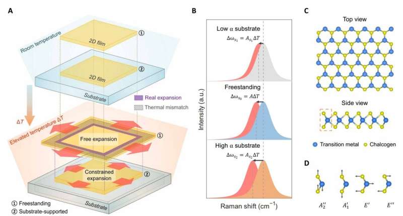
Because 2D materials are so small—perhaps just a few microns in size—standard tools aren't sensitive enough to directly measure their expansion. Plus, the materials are so thin they must be bonded to a substrate such as silicon or copper. If the 2D material and its substrate have different TECs, they will expand differently when temperatures increase, which causes thermal stress.
For instance, if a 2D material is bonded to a substrate with a higher TEC, when the device is heated the substrate will expand more than the 2D material, which stretches it. This makes it difficult to measure the actual TEC of a 2D material since the substrate affects its expansion.
The researchers overcame these problems by focusing on the atoms that make up the 2D material. When a material is heated, its atoms vibrate at a lower frequency and move farther apart, which causes the material to expand. They measure these vibrations using a technique called micro-Raman spectroscopy, which involves hitting the material with a laser. The vibrating atoms scatter the laser's light, and this interaction can be used to detect their vibrational frequency.
But as the substrate expands or compresses, it impacts how the 2D material's atoms vibrate. The researchers needed to decouple this substrate effect to zero in on the material's intrinsic properties. They did this by measuring the vibrational frequency of the same 2D material on three different substrates: copper, which has a high TEC; fused silica, which has a low TEC; and a silicon substrate dotted with tiny holes. Because the 2D material hovers above the holes on the latter substrate, they can perform measurements on these tiny areas of freestanding material.
The researchers then placed each substrate on a thermal stage to precisely control the temperature, heated each sample, and performed micro-Raman spectroscopy.
"By performing Raman measurements on the three samples, we can extract something called the temperature coefficient that is substrate dependent. Using these three different substrates, and knowing the TECs of the fused silica and the copper, we can extract the intrinsic TEC of the 2D material," Zhong explains.
A curious result
They performed this analysis on several 2D materials and found that they all matched theoretical calculations. But the researchers saw something they didn't expect: 2D materials fell into a hierarchy based on the elements that comprise them. For instance, a 2D material that contains molybdenum always has a greater TEC than one which contains tungsten.
The researchers dug deeper and learned that this hierarchy is caused by a fundamental atomic property known as electronegativity. Electronegativity describes the tendency for atoms to pull or extract electrons when they bond. It is listed on the periodic table for each element.
They found that the larger the difference between electronegativities of elements that form a 2D material, the lower the material's thermal expansion coefficient will be. An engineer could use this method to quickly estimate the TEC for any 2D material, rather than relying on complex calculations that typically must be crunched by a supercomputer, says Zhong.
"An engineer can just search the periodic table, get the electronegativities of the corresponding materials, plug them into our correlation equation and within a minute they can have a reasonably good estimation of the TEC. This is very promising for rapid materials selection for engineering applications," Zhang says.
Moving forward, the researchers want to apply their methodology to many more 2D materials, perhaps building a database of TECs. They also want to use micro-Raman spectroscopy to measure TECs of heterogenous materials, which combine multiple 2D materials. And they hope to learn the underlying reasons thermal expansion of 2D materials is different from that of bulk materials.

 Previous page
 Back to top


