From microscopes and cameras to
night vision devices and optical fiber communications, photodetectors have a
wide array of applications. Photodetectors capture and convert light into
electrical signals but are often limited to detecting a narrow part of the
wavelength spectrum. The materials used to make these devices often hamper
efforts to make improved broadband nanoscale photodetectors.
A new device from San Francisco State University Physics & Astronomy Associate Professor AKM Newaz and his graduate student Hon-Loen Sinn may overcome some of these challenges. In a new Advanced Photonics Research paper, the team and their Stanford University collaborators describe the impressive properties of their photodetector that has improved sensitivity in the ultraviolet (UV) to near-infrared light range. They've submitted a provisional patent for their device and are working on the main patent application.
"A UV [ultraviolet] photodetector is very useful for [a range of applications from] biology to space astronomy to fire monitors. All these current communication channels [use] the visible range and infrared," Newaz said. "We don't have many higher efficiency UV photodetector devices, so people don't use UV."
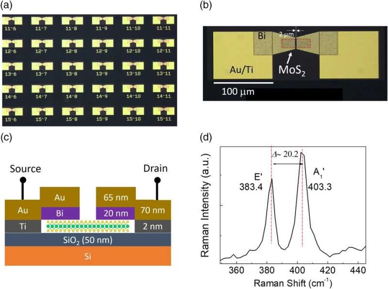
Newaz's lab studies atomically thin semiconductor materials such as molybdenum disulfide (MoS2) to create broadband nanoscale photodetectors. Although MoS2 shows promise, it has defects when interfacing with metals like gold found in some devices. Recent research suggests introducing semimetals like tin or bismuth may mitigate these interfering defects, Newaz explained.
"When you use regular gold, you have a high resistance, and the high resistance comes from an interface defect-related barrier known as Schottky barrier. … But when you use a bismuth semimetal, you can show that the barrier disappears," he said. "By analyzing the data, you can show that the interface with bismuth is kind of free of Schottky barrier."
Though this alone is not new, the San Francisco State team is among the first to describe the optoelectronic properties—such as measurement of optical-to-electrical conversion, response time and scalability—of a bismuth-MoS2 device.
The researchers showed that introducing bismuth made their device 30,000 times more photoresponsive than photodetectors with gold alone. Testing their photodetector, they saw that the device was most sensitive in the UV range and was responsive over a wide wavelength range (380—1,000 nm). Not only did sensitivity improve, but the device was more sensitive with a low power level.
"It's telling us that you can make an extremely sensitive photodetector by using a one-atom thick semiconductor," Newaz said. "You have a better result if you use bismuth than typical gold or other noble metals."
Another key finding, he added, was that their device is fast. It works at about 10 kilohertz, which is 10 to 100 times faster than other devices.
"Using semimetal, industry is already thinking about going to extremely small size [with devices] and are planning to use MoS2 and bismuth as a transistor," Newaz explained. "We are showing that [these same materials] can also work as a very good photodetector. They can be merged together so some part can work as an extremely sensitive communication tool via light and then communicate the signals to the transistor part."
Newaz suspects that their device might actually be faster and its speed may fall in the megahertz or gigahertz range, which means the device could be over a thousand times faster than the 10 kilohertz they showed experimentally in this paper. A faster device is necessary for faster data communications in which the photodetector converts fast optical signal into a fast electrical signal.
"We submitted a patent for our atom-thick semiconductors," Newaz said. "This is a very proud moment for my lab that a student's research results in a patent application and a publication in a top tier journal."
Newaz is excited about this work, particularly because it showcases the caliber of research performed by SF State students, noting that the lead author was a master's student in his lab. "This publication is Ph.D.-student quality work, and it was done by a master's student at SF State," he added.

 Previous page
 Back to top


