A new publication from Opto-Electronic
Advances discusses high performance integrated photonic-circuit-based on
inverse design method.
With the explosive growth of information and data, photonic integrated circuits and chips have higher requirements for ultra-fast response time, ultra-small size, ultra-low energy threshold and high integration density. The photonic integrated circuit is composed of micro/nano structure and uses photon instead of electron as information carrier. Traditional photonic integrated circuits based on von Neumann like structures mainly use regular or periodic structures, such as micro-ring resonators, photonic crystals (PC), surface plasmon polaritons (SPPs) and metamaterials, etc. Such dielectric structures usually need a large size, causing the overall size of the circuit large, usually reaches hundreds of microns. Although the size of SPPs circuits is small, their huge transmission loss is still a tremendous difficulty to limit the realization of low energy consumption. To realize complex functions, traditional devices usually adopt nonlinear material. However, the contradiction between the ultrafast response and the large nonlinear coefficient of nonlinear materials leads to the contradiction between ultrafast response and ultra-low energy consumption. Until now, it is still a huge challenge to realize an integrated photonic circuit with high performance of ultrahigh density integration, ultrafast response and ultra-low energy consumption.
Traditionally, the designs of micro/nano-devices are mainly based on finite difference time domain method (FDTD) and finite element method (FEM) through solving the maxwell's equations, but the methods usually involve a long process through repeated calculation to optimize structural parameters by manually adjusting the parameters of nanostructures, such as the width of the waveguides, the diameter of air holes and the size of the micro-rings, etc. Inverse design method, using algorithm technique to calculate unknown optical structures or optimize known structures based on expected functional characteristics, is more suitable for the design and optimization of optical micro/nano-structures. The inverse design method can optimize the performance of a single device or enrich the function of the whole circuit, such as high-performance grating couplers, wavelength demultiplexer, power splitter, polarization beam splitter, etc. The inverse design method is more suitable for the design and optimization of photonic integrated circuits and is expected to break through the bottleneck of on-chip information processing capability.
The authors of this paper proposed and experimentally demonstrated an approach based on inverse design method to realize a high-density, ultrafast and ultra-low energy consumption integrated photonic circuit. The research group improved the inverse design algorithm to meet the demand of optimizing the performance of the whole circuit. The advantage of the algorithm was the existence of adjoint field distribution. The adjoint method required the dielectric constant "drop one step" along the gradient descent direction, the gradient was calculated according to the objective function, and the dielectric constant was iterated along the gradient direction.
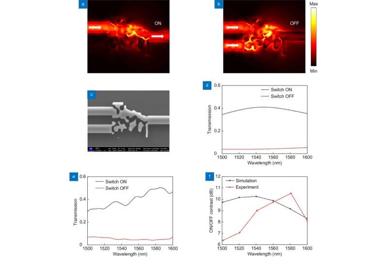
The circuit composed three devices with two all-optical switches controlling the input states of an XOR logic gate. The feature size of the whole circuit was only 2.5 μm×7 μm, and that of a single device was 2 μm×2 μm. The distance between two adjacent devices was as small as 1.5 μm, within wavelength magnitude scale. Through the scattering of the inverse-design disordered nanostructures, the mode field distribution of signal light was changed. When the signal light input, it can transmit through the disordered nanostructures. When the control light input, the mode field of two lights coherently overlay, which changed the mode field distribution of the signal light and the control light, thus the signal light cannot transmitted through the disordered nanostructures. The theoretical response time of the inverse-design all-optical switch was 100 fs, and the threshold energy of control light was 10 fJ/bit, equal to the signal light for the all-optical switch. The response time of the logic gate was 20 fs. The research group also considered the crosstalk problem through the whole optimizing process of the integrated circuit. The circuit not only integrated three devices but also realized a function of identifying two-digit logic signal results. This work provides a new idea for the design of ultrafast, ultra-low energy consumption and ultra-high density integrated photonic circuit.

 Previous page
 Back to top


