Nanomolding of topological
nanowires could speed the discovery of new materials for applications such as
quantum computing, microelectronics and clean-energy catalysts, according to an
article co-authored by Judy Cha, professor of materials science and engineering
at Cornell.
Topological materials are valued for their unique ability to possess different properties at their surfaces and edges, and these surface properties can be enhanced by engineering the materials at the nanoscale. The challenge for scientists is that traditional methods of fabricating nanowires are slow and don't offer a high level of precision.
"Theorists have predicted about a quarter of all known inorganic crystals may be topological," Cha said. "We're talking tens of thousands of compounds, so the conventional method of making these crystals is just incompatible in terms of screening them to look for test topological materials for specific applications."
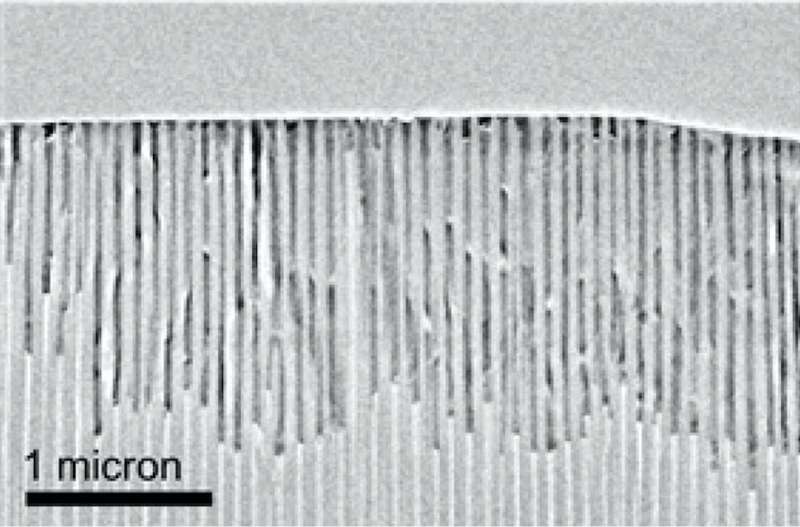
But nanomolding, in which a bulk polycrystalline feedstock is pressed into a nanostructured mold at an elevated temperature to form nanowires, could provide a solution. Writing in APL Materials, Cha and postdoctoral associate Mehrdad Kiani explain nanomolding offers several advantages over existing synthesis methods for nanoscale materials.
"Unlike traditional top-down and bottom-up fabrication methods, nanomolding requires minimal optimization of experimental parameters and can work on a wide variety of topological compounds, thus enabling high throughput fabrication of topological nanowires. The fabricated nanowires are single crystalline and defect-free and can have high aspect ratios greater than 1,000," write Cha and Kiani.
Nanomolding had previously been used for metallic material systems, but Cha and her research group are one of the first to expand its application to topological materials. And while, in principle, nanomolding delivers all the traits wanted in a topological nanowire, exactly how and why the method is so successful is still not fully understood—a knowledge gap that the Cha Group is working to fill.
Current research projects in the Cha Group include measuring the electrical properties of nanomolded topological nanowires to benchmark against nanowires produced with other techniques, and studying atomic diffusion and mechanical motions of atoms during the molding process. Cha is also welcoming collaborators interested in nanowire versions of compounds that they are researching.
The research was also featured in AIP Scilight.

 Previous page
 Back to top


