A new type of active pixel sensor
that uses a novel two-dimensional material may both enable ultra-sharp
cellphone photos and create a new class of extremely energy-efficient Internet
of Things (IoT) sensors, according to a team of Penn State researchers.
"When people are looking for a new phone, what are the specs that they are looking for?" said Saptarshi Das, associate professor of engineering science and mechanics and lead author of the study published Nov. 17 in Nature Materials. "Quite often, they are looking for a good camera, and what does a good camera mean to most people? Sharp photos with high resolution."
Most people just snap a photo of a friend, a family gathering, or a sporting event, and never think about what happens "behind the scenes" inside the phone when one snaps a picture. According to Das, there is quite a bit happening to enable you to see a photo right after you take it, and this involves image processing.
"When you take an image, many of the cameras have some kind of processing that goes on in the phone, and in fact, this sometimes makes the photo look even better than what you are seeing with your eyes," Das said. "These next generation of phone cameras integrate image capture with image processing to make this possible, and that was not possible with older generations of cameras."
However, the great photos in the newest cameras have a catch—the processing requires a lot of energy.
"There's an energy cost associated with taking a lot of images," said Akhil Dodda, a graduate research assistant at Penn State at the time of the study who is now a research staff member at Western Digital, and co-first author of the study.
"If you take 10,000 images, that is fine, but somebody is paying the energy costs for that. If you can bring it down by a hundredfold, then you can take 100 times more images and still spend the same amount of energy. It makes photography more sustainable so that people can take more selfies and other pictures when they are traveling. And this is exactly where innovation in materials comes into the picture."
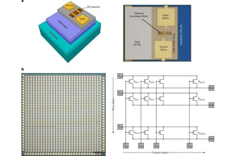
The innovation in materials outlined in the study revolves around how they added in-sensor processing to active pixel sensors to reduce their energy use. So, they turned to a novel 2D material, which is a class of materials only one or a few atoms thick, molybdenum disulfide. It is also a semiconductor and sensitive to light, which makes it ideal as a potential material to explore for low-energy in-sensor processing of images.
"We found that molybdenum disulfide has very good photosensitive response," said Darsith Jayachandran, graduate research assistant in engineering and mechanics and co-first author of the study. "From there, we tested it for the other properties we were looking for."
These properties included sensitivity to low light, which is important for the dynamic range of the sensor. The dynamic range refers to the ability to "see" objects in both low light such as moonlight and bright light such as sunlight. The human eye can see stars at night better than most cameras due to having superior dynamic range.
Molybdenum disulfide also demonstrated strong signal conversion, charge-to-voltage conversion and data transmission capabilities. This makes the material an ideal candidate to enable an active pixel sensor that can do both light sensing and in-sensor image processing.
"From there, we put the sensors into an array," Jayachandran said. "There are 900 pixels in a nine square millimeter array we developed, and each pixel is about 100 micrometers. They are much more sensitive to light than current CMOS sensors, so they do not require any additional circuitry or energy use. So, each pixel requires much less energy to operate, and this would mean a better cellphone camera that uses a lot less battery."
The dynamic range and image processing would enable users to take sharp photos in a variety of adverse conditions for photography, according to Das.
"For example, you could take clearer photos of friends outside at night or on a rainy or foggy day," Das said. "The camera could do denoising to clear up the fog and the dynamic range would enable say a night photo of a friend with stars in the background."
Das noted that the three main facilities in the Materials Research Institute were instrumental in creating and testing the material.
"The 2D materials we used for the experiments were grown at the Two-Dimensional Crystal Consortium facility at Penn State which is a National Science Foundation Materials Innovation Platform (MIP) facility, the characterization of the material was done in the Materials Characterization Laboratory, and we also used the cleanrooms in the Nanofabrication Laboratory," Das said. "Having easy access to these facilities right on campus played a major role in making this research successful."
Along with enabling a top-rate phone camera in the future, the team also envisions their improved sensor technology could have other applications. This would include better light sensors for Internet of Things and Industry 4.0 applications. Industry 4.0 is the term for a growing movement that combines traditional industry practices and cutting-edge digital technology such as the Internet of Things, cloud data storage, and artificial intelligence/machine learning. The goal is to improve manufacturing by developing more efficient processes and practices through intelligent automation, and sensors are key.
"Sensors that can see through machines while in operation and identify defects are very important in the IoT," Dodda said. "Conventional sensors consume a lot of energy so that is a problem, but we developed an extremely energy efficient sensor that enables better machine learning, etc. and saves a lot in energy costs."

 Previous page
 Back to top


