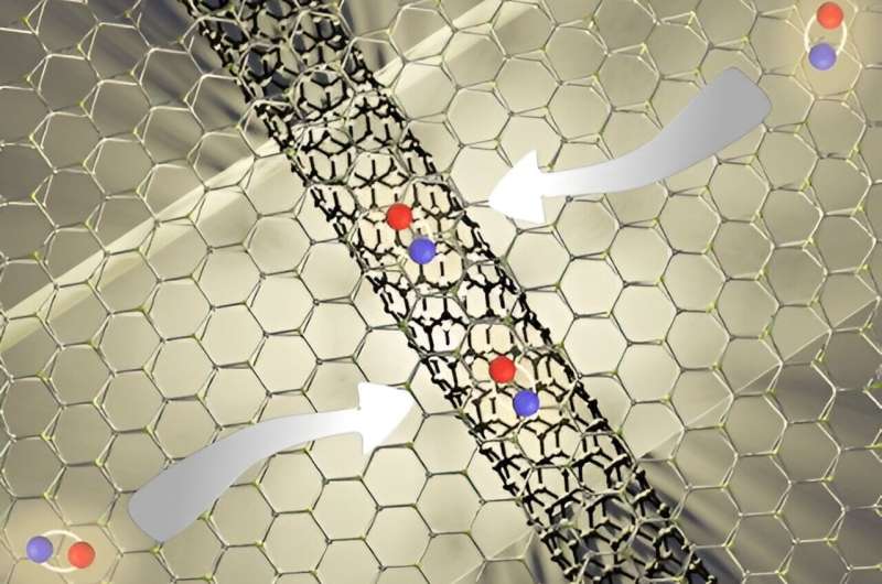
A flat sheet of atoms can act as
a kind of antenna that absorbs light and funnels its energy into carbon
nanotubes, making them glow brightly. This advance could aid the development of
tiny future light-emitting devices that will exploit quantum effects.
Carbon nanotubes resemble very thin, hollow wires with a diameter of just a nanometer or so. They can generate light in various ways. For example, a laser pulse can excite negatively charged electrons within the material, leaving positively charged "holes." These opposite charges can pair up to form an energetic state known as an exciton, which may travel relatively far along a nanotube before releasing its energy as light.
In principle, this phenomenon could be exploited to make highly efficient nanoscale light-emitting devices.
Unfortunately, there are three obstacles to using a laser to generate excitons within carbon nanotubes. First, a laser beam is typically 1,000 times wider than a nanotube, so very little of its energy is actually absorbed by the material. Second, the light waves must align perfectly with the nanotube to deliver their energy effectively. Finally, the electrons in a carbon nanotube can only absorb very specific wavelengths of light.
To overcome these limitations, a team led by Yuichiro Kato of the RIKEN Nanoscale Quantum Photonics Laboratory turned to another class of nanomaterials, known as 2D materials. These flat sheets are just a few atoms thick, but they can be much wider than a laser beam, and are far better at converting laser pulses into excitons.
The researchers grew carbon nanotubes over a trench carved from an insulating material. They then placed an atomically thin flake of tungsten diselenide on top of the nanotubes. When laser pulses hit this flake, they generated excitons that moved into the nanotube and along its length, before releasing light of a longer wavelength than the laser. It took just one trillionth of a second for each exciton to pass from the 2D material into the nanotube.
The paper is published in the journal Nature Communications.
By testing nanotubes with a range of different structures that affect crucial energy levels within the material, the researchers identified ideal nanotube forms that facilitate the transfer of excitons from the 2D material.
Based on this result, they intend to use band engineering—a useful concept in semiconducting engineering to realize devices with superior properties—at the atomically thin scale. "When band engineering is applied to low-dimensional semiconductors, new physical properties and innovative functionalities are expected to emerge," says Kato.
"We hope to utilize this concept to develop photonic and optoelectronic devices that are just a few atomic layers thick," adds Kato. "If we can shrink them to the atomically thin limit, we expect novel quantum effects to emerge, which may become useful for future quantum technologies."

 Previous page
 Back to top


