Imagine placing
an object under a microscope and pressing a button to rearrange the surface
atoms with atomic-scale precision. This once sci-fi scenario is now a reality
thanks to pioneering research published in Applied Surface Science.
"Our laser method provides atomic-level control over diamond surfaces in a standard air environment," says lead researcher Dr. Mojtaba Moshkani.
"This level of precision is typically only possible with large, complex vacuum equipment. The ability to achieve it with a simple laser process is truly remarkable."
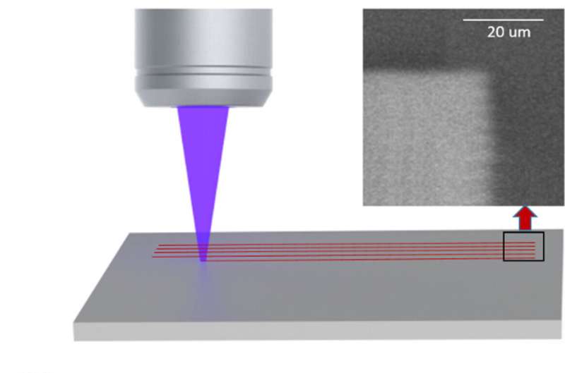
Harnessing the power of deep ultraviolet (UV) laser light, researchers have developed a technique for precise surface processing of diamonds. The method allows for the controlled removal of as little as 1 percent of a single atomic layer, offering unprecedented control over the structure and properties of the diamond surface.
Using a deep ultraviolet laser, the team demonstrated how precisely delivered pulses of light can trigger localized chemical reactions on a diamond surface. The reaction, driven by a two-photon process, removes carbon atoms selectively from the top atomic layer.
This breakthrough is set to transform applications in electronics, quantum devices, and advanced manufacturing, where even minor adjustments to the configuration of surface atoms can significantly enhance device performance.
Enhanced conductivity
One of the most exciting findings was a dramatic increase in diamond surface conductivity—up to seven times higher—after laser treatment. This enhancement was independently confirmed by collaborators at MIT Lincoln Laboratory.
"We were amazed that such a minor adjustment to the surface could yield such a substantial boost in conductivity," says team lead Professor Richard Mildren.
This result is a critical step toward addressing challenges in making diamond a viable material for semiconductors. The unique properties of diamonds, including high thermal conductivity and resistance to electrical breakdown, make it an ideal candidate for high-power, high-frequency electronic devices.
Speed and scalability for industry
The technique is not only precise but also fast. In current experiments, the laser removed 1 percent of a monolayer in just 0.2 milliseconds. This makes it a promising candidate for large-scale industrial applications, such as wafer processing.
"We've shown that the process is both rapid and scalable," adds Dr. Moshkani. "It's a compelling option for industries requiring advanced material processing."
Implications for quantum technologies
Beyond electronics, this discovery has far-reaching implications for quantum technologies. Diamond surfaces play a critical role in stabilizing quantum states, such as those used in quantum computers. The ability to engineer diamond surfaces with atomic precision could become an essential tool for researchers and industry alike.
"This is just the beginning," says Professor Mildren. "We are excited to explore how this technique can be optimized further to unlock the full potential of diamonds in electronics, quantum technologies, and beyond."

 Previous page
 Back to top


