 The number of transistors it is possible to squeeze in to a chip for a fixed cost doubles every two years
First outlined by Gordon Moore, co-founder of Intel
Published in Electronics Magazine on
For more than 40 years the silicon industry has delivered ever faster, cheaper chips.
The advances have underpinned everything from the rise of mobile phones to digital photography and portable music players.
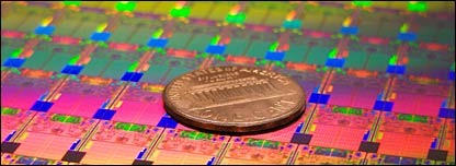
Chip-makers have been able to deliver many of these advances by shrinking the components on a chip.
By making these building blocks, such as transistors, smaller they have become faster and firms have been able to pack more of them into the same area.
But according to many industry insiders this miniaturisation cannot continue forever.
|
The number of transistors it is possible to squeeze in to a chip for a fixed cost doubles every two years First outlined by Gordon Moore, co-founder of Intel Published in Electronics Magazine on |
"The consensus in the industry is that we can do that shrink for about another ten years and then after that we have to figure out new ways to bring higher capability to our chips," said Professor Stanley Williams of Hewlett Packard.
Even Gordon Moore, the founder of Intel and the man that gave his name to the law that dictates the industry is progression, admits that it can only go on for a few more years.
"
Tiny tubes
As a result, researchers around the world are engaged in efforts to allow the industry to continue delivering the advances that computer users have come to expect.
Key areas include advanced fabrication techniques, building new components and finding new materials to augment silicon.
Already new materials are creeping into modern chips.
As components have shrunk critical elements of the transistors, known as gate dielectrics, do not perform as well allowing currents passing through the transistors to leak, reducing the effectiveness of the chip.
To overcome this, companies have replaced the gate dielectrics, previously made from silicon dioxide, with an oxide based on the metal hafnium.
The material is development and integration into working components has been described by Dr Moore as "the biggest change in transistor technology" since the late 1960s.
But IBM researchers are working on materials that they believe offer even bigger advances.
"Carbon nanotubes are a step beyond [hafnium]," explained Dr Phaedon Avouris of the company.
design
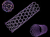
Carbon nanotubes are tiny straw-like molecules less than 2 nanometres (billionths of a metre) in diameter, 50,000 times thinner than a strand of a human hair.
"They are a more drastic change but still preserve the basic architecture of field effect transistors."
These transistors are the basic building blocks of most silicon chips.
Dr Avouris believes they can be used to replace a critical element of the chip, known as the channel.
Today this is commonly made of silicon and is the area of the transistor through which electrons flow.
Chip makers are constantly battling to make the channel length in transistors smaller and smaller, to increase the performance of the devices.
Carbon nanotube is small size and "superior" electrical properties should be able to deliver this, said Dr Avouris.
Crucially, he also believes the molecules can be integrated with traditional silicon manufacturing processes, meaning the technology would more likely be accepted by an industry that has spent billions perfecting manufacturing techniques.
The team have already shown off working transistors and are currently working on optimising their production and integration into working devices.
Tiny improvement
Professor Williams, at Hewlett Packard is also working on technology that could be incorporated into the future generations of chips.
As well as exploring optical computing - using particles of light instead of electrons to significantly increase the speed of today is computers - he is building new electronic components for chips called memristors. 
He says it would be the "fourth" basic element to build circuits with, after capacitors, resistors and inductors.
"Now we have this type of device we have a broader palette with which to paint our circuits," said Professor Williams.
Professor Williams and his team have shown that by putting two of these devices together - a configuration called a crossbar latch - it could do the job of a transistor. (Pic. carbon nanatubes)
"A cross bar latch has the type of functionality you want from a transistor but it is working with very different physics," he explained.
Crucially, these devices can also be made much smaller than a transistor.
"And as they get smaller they get better," he said.
Professor Williams and his team are currently making prototype hybrid circuits - built of memristors and transistors - in a fabrication plant in
"We want to keep the functional equivalent of
By Jonathan Fildes

 Previous page
 Back to top


