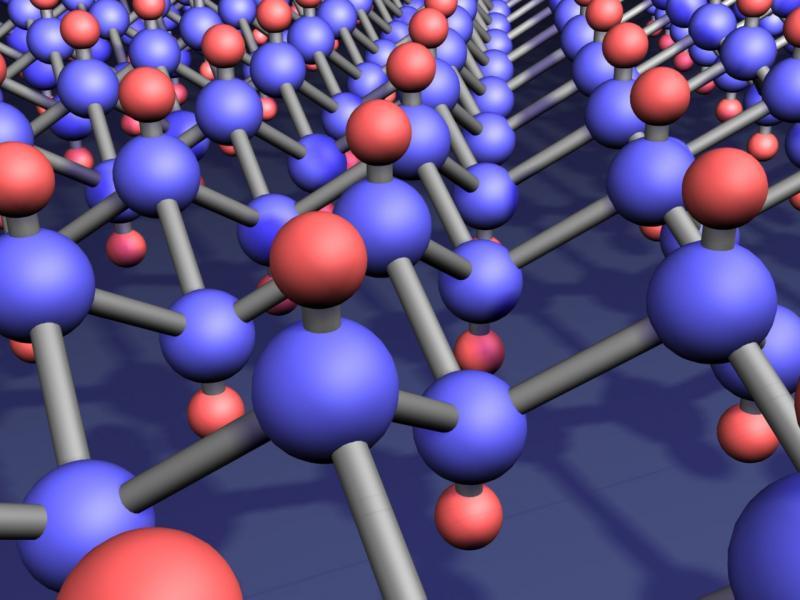
Combining wonder material graphene with other stunning one-atom thick materials could create the next generation of solar cells and optoelectronic devices, scientists have revealed.
 University of Manchester and National University of Singapore researchers have shown how building multi-layered heterostructures in a three-dimensional stack can produce an exciting physical phenomenon exploring new electronic devices.
The breakthrough, published in Science, could lead to electric energy that runs entire buildings generated by sunlight absorbed by its exposed walls; the energy can be used at will to change the transparency and reflectivity of fixtures and windows depending on environmental conditions, such as temperature and brightness.
The isolation of graphene, by University of Manchester Nobel Laureates Professor Andre Geim and Professor Kostya Novoselov in 2004, led to the discovery of the whole new family of one-atom-thick materials.
Graphene is the world's thinnest, strongest and most conductive material, and has the potential to revolutionise a huge number of diverse applications; from smartphones and ultrafast broadband to drug delivery and computer chips. The isolation of graphene also led to the discovery of a whole new family of one-atom-thick materials.
Collectively, such 2D crystals demonstrate a vast range of superlative properties: from conductive to insulating, from opaque to transparent. Every new layer in these stacks adds exciting new functions, so the heterostructures are ideal for creating novel, multifunctional devices.
One plus one is greater than two -- the combinations of 2D crystals allow researchers to achieve functionality not available from any of the individual materials.
The Manchester and Singapore researchers expanded the functionality of these heterostructures to optoelectronics and photonics. By combining graphene with monolayers of transition metal dichalcogenides (TMDC), the researchers were able to created extremely sensitive and efficient photovoltaic devices. Such devices could potentially be used as ultrasensitive photodetectors or very efficient solar cells.
In these devices, layers of TMDC were sandwiched between two layers of graphene, combining the exciting properties of both 2D crystals. TMDC layers act as very efficient light absorbers and graphene as a transparent conductive layer. This allows for further integration of such photovoltaic devices into more complex, more multifunctional heterostructures.
Professor Novoselov said: "We are excited about the new physics and new opportunities which are brought to us by heterostructures based on 2D atomic crystals. The library of available 2D crystals is already quite rich, covering a large parameter space.
"Such photoactive heterostructures add yet new possibilities, and pave the road for new types of experiments. As we create more and more complex heterostructures, so the functionalities of the devices will become richer, entering the realm of multifunctional devices."
University of Manchester researcher and lead author Dr Liam Britnell added: "It was impressive how quickly we passed from the idea of such photosensitive heterostructures to the working device. It worked practically from the very beginning and even the most unoptimised structures showed very respectable characteristics"
Professor Antonio Castro Neto, Director of the Graphene Research Centre at the National University of Singapore added: "We were able to identify the ideal combination of materials: very photosensitive TMDC and optically transparent and conductive graphene, which collectively create a very efficient photovoltaic device.
"We are sure that as we research more into the area of 2D atomic crystals we will be able to identify more of such complimentary materials and create more complex heterostructures with multiple functionalities. This is really an open field and we will explore it."
Dr Cinzia Casiraghi, from The University of Manchester, added: "Photosensitive heterostructures would open a way for other heterostructures with new functionalities. Also, in future we plan for cheaper and more efficient heterostructure for photovoltaic applications."

 Previous page
 Back to top


