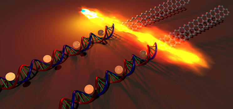
Graphene is a sheet of carbon atoms arrayed in a honeycomb pattern, just a single atom thick. It could be a better semiconductor than silicon -- if we could fashion it into ribbons 20 to 50 atoms wide. Could DNA help?
 DNA is the blueprint for life. Could it also become the template for making a new generation of computer chips based not on silicon, but on an experimental material known as graphene?
That's the theory behind a process that Stanford chemical engineering professor Zhenan Bao reveals in Nature Communications.
Bao and her co-authors, former post-doctoral fellows Anatoliy Sokolov and Fung Ling Yap, hope to solve a problem clouding the future of electronics: consumers expect silicon chips to continue getting smaller, faster and cheaper, but engineers fear that this virtuous cycle could grind to a halt.
Why has to do with how silicon chips work.
Everything starts with the notion of the semiconductor, a type of material that can be induced to either conduct or stop the flow of electricity. Silicon has long been the most popular semiconductor material used to make chips.
The basic working unit on a chip is the transistor. Transistors are tiny gates that switch electricity on or off, creating the zeroes and ones that run software.
To build more powerful chips, designers have done two things at the same time: they've shrunk transistors in size and also swung those gates open and shut faster and faster.
The net result of these actions has been to concentrate more electricity in a diminishing space. So far that has produced small, faster, cheaper chips. But at a certain point, heat and other forms of interference could disrupt the inner workings of silicon chips.
"We need a material that will let us build smaller transistors that operate faster using less power," Bao said.
Graphene has the physical and electrical properties to become a next-generation semiconductor material -- if researchers can figure out how to mass-produce it.
Graphene is a single layer of carbon atoms arranged in a honeycomb pattern. Visually it resembles chicken wire. Electrically this lattice of carbon atoms is an extremely efficient conductor.
Bao and other researchers believe that ribbons of graphene, laid side-by-side, could create semiconductor circuits. Given the material's tiny dimensions and favorable electrical properties, graphene nano ribbons could create very fast chips that run on very low power, she said.
"However, as one might imagine, making something that is only one atom thick and 20 to 50 atoms wide is a significant challenge," said co-author Sokolov.
To handle this challenge, the Stanford team came up with the idea of using DNA as an assembly mechanism.
Physically, DNA strands are long and thin, and exist in roughly the same dimensions as the graphene ribbons that researchers wanted to assemble.
Chemically, DNA molecules contain carbon atoms, the material that forms graphene.
The real trick is how Bao and her team put DNA's physical and chemical properties to work.
The researchers started with a tiny platter of silicon to provide a support (substrate) for their experimental transistor. They dipped the silicon platter into a solution of DNA derived from bacteria and used a known technique to comb the DNA strands into relatively straight lines.
Next, the DNA on the platter was exposed to a copper salt solution. The chemical properties of the solution allowed the copper ions to be absorbed into the DNA.
Next the platter was heated and bathed in methane gas, which contains carbon atoms. Once again chemical forces came into play to aid in the assembly process. The heat sparked a chemical reaction that freed some of the carbon atoms in the DNA and methane. These free carbon atoms quickly joined together to form stable honeycombs of graphene.
"The loose carbon atoms stayed close to where they broke free from the DNA strands, and so they formed ribbons that followed the structure of the DNA," Yap said.
So part one of the invention involved using DNA to assemble ribbons of carbon. But the researchers also wanted to show that these carbon ribbons could perform electronic tasks. So they made transistors on the ribbons.
"We demonstrated for the first time that you can use DNA to grow narrow ribbons and then make working transistors," Sokolov said.
The paper drew praise from UC Berkeley associate professor Ali Javey, an expert in the use of advanced materials and next-generation electronics.
"This technique is very unique and takes advantage of the use of DNA as an effective template for controlled growth of electronic materials," Javey said. "In this regard the project addresses an important research need for the field."
Bao said the assembly process needs a lot of refinement. For instance, not all of the carbon atoms formed honeycombed ribbons a single atom thick. In some places they bunched up in irregular patterns, leading the researchers to label the material graphitic instead of graphene.
Even so, the process, about two years in the making, points toward a strategy for turning this carbon-based material from a curiosity into a serious contender to succeed silicon.
"Our DNA-based fabrication method is highly scalable, offers high resolution and low manufacturing cost," said co-author Yap. "All these advantages make the method very attractive for industrial adoption."
The experiment was supported in part by the National Science Foundation and the Stanford Global Climate and Energy Program.

 Previous page
 Back to top


