Printers are becoming more and more versatile. Now they can even print sensors and electronic components on 2D and 3D substrates. A new, robot-assisted production line allows the process to be automated.

These days, no office is complete without a printer. But digital printing technologies also play an important role in microelectronics, microsystems engineering and sensor systems. Researchers at the Fraunhofer Institute for Manufacturing Technology and Advanced Materials IFAM in Bremen use various printing methods to produce electronic components and sensors. The tiny resistors, transistors, circuit paths and capacitors are first designed on screen and then deposited directly onto two- and three-dimensional substrates, for instance circuit boards. Instead of the usual paper inks, the scientists use what are known as "functional inks" -- electronic materials in liquid or paste form. The range of potential uses for printed electronics is wide -- from the electronic circuits in digital thermometers to flexible sheets of solar cells and smart packaging with built-in sensors.
To automate the process of applying printed electronics to components with flat and three-dimensional surfaces, the IFAM scientists have set up a robot-assisted production line that allows different printing methods to be combined in a single run. Modules for silk-screen, inkjet, dispenser, and aerosol-jet printing are integrated in the production unit. "The production line with its central robotic unit, component feeders, printing systems and heat treatment furnaces enables us to functionalize surfaces on a near-industrial scale," says Dr. Volker Zöllmer, head of the Functional Structures department at IFAM.
The availability of different technologies in one system makes it possible to print structures of different surface areas, widths, and thicknesses on the substrate. Aerosol-jet printing, for instance, enables the researchers to deposit extremely fine structures with a width of only 10 micrometers onto the component. In this non-contact process, the conductive ink is transformed into an aerosol using compressed air (pneumatic spraying), and then fed to the print head through a fine tube. The print head focuses the aerosol jet on the surface of the substrate, which doesn't necessarily have to be flat or smooth -- even curved surfaces can be printed on using this method. It is also possible to vary the thickness of the printed features and create multilayer structures. "For example, as well as laying down circuits on a circuit board, we can also provide it with a corrosion-resistant coating," says Zöllmer.
So how exactly does this printing process work? After the control software has been programmed for the desired end product, by defining the printing methods required and the order in which they are to be executed, the robot picks up the substrate, for instance a bare circuit board, and dispatches it to the first printing station. If the task requires integrating 200-micrometer-wide circuit paths in the substrate, it is first sent to the dispenser, a piezoelectric dosing system. The dispenser contains a valve that allows the precise volume and droplet size of the viscous medium -- e.g. an electrically conductive adhesive -- to be applied. If the conductor is to be connected to a sensor, the circuit board is then routed to the aerosol-jet printer. This high-resolution device prints the sensors. The circuit board then passes through other printers, depending on the application, before finally undergoing heat treatment in the furnace, in order to obtain the desired performance characteristics. The system is capable of printing on substrates up to the size of a DIN-A3 sheet of paper, and can process components with a height of several centimeters.
Functionalized surfaces to order
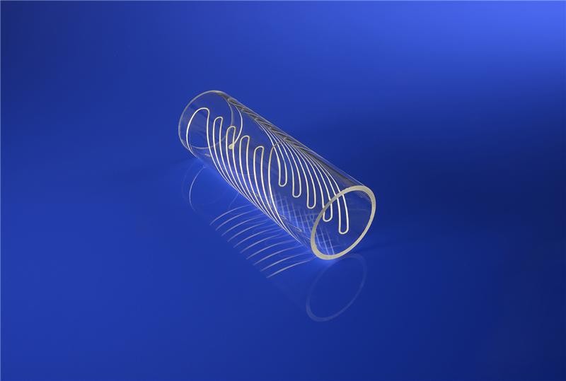
The choice of materials that can be used as substrates or functional inks is almost unlimited. The inks employed by the IFAM specialists include metals, ceramics, electrically conductive polymers, and even biomaterials such as proteins and enzymes. Depending on the application, these media are deposited on substrates made of glass, textiles, metals, ceramic plates, and many other materials. "The new production line enables us to process a wide range of different materials and combine them in many different ways to meet the customer's requirements. This includes designing components capable of providing entirely new functions -- such as window panes with integrated sensors for measuring temperature." Zöllmer adds. "Printed sensors can also be used to monitor building components, providing early warning of crack formation and other structural damage. They could also be useful in the car industry, where strain gages printed on aluminum surfaces by means of aerosol-jet printing could provide an early indication of material fatigue in body components."
The robot-assisted production line also helps to shorten development lead times. In the past, to provide components with sensor functions, it was often necessary to integrate the sensors in the component after it had been manufactured -- a time-consuming process. Depending on the application, the IFAM researchers can achieve the same result in a matter of seconds or minutes by printing fully functionalized components. This offers advantages to many sectors of industry, including car manufacturing and aerospace, and also microsystems engineering. "We can help industry to streamline its product development processes, by manufacturing prototypes and small batches using our production line," says Zöllmer. The modular production line also provides scope for customers to add their own processes.

 Previous page
 Back to top


