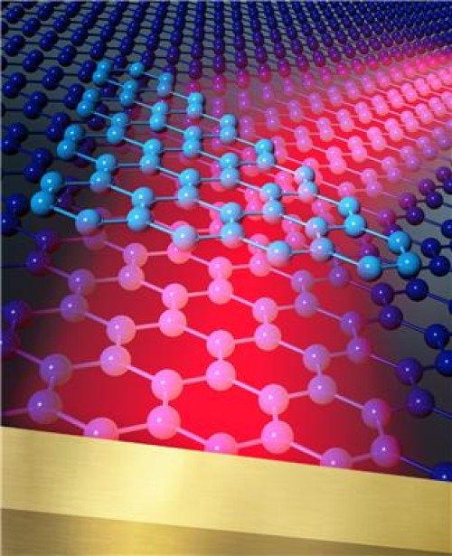
Researchers from CIC nanoGUNE, in collaboration with ICFO and Graphenea, introduce a platform technology based on optical antennas for trapping and controlling light with the one-atom-thick material graphene. The experiments show that the dramatically squeezed graphene-guided light can be focused and bent, following the fundamental principles of conventional optics. The work, published yesterday in Science, opens new opportunities for smaller and faster photonic devices and circuits.
 Optical circuits and devices could make signal processing and computing much faster. "However, although light is very fast it needs too much space," explains Rainer Hillenbrand, Ikerbasque Professor at nanoGUNE and UPV/EHU. In fact, propagating light needs at least the space of half its wavelength, which is much larger than state-of-the-art electronic building blocks in our computers. For that reason, a quest for squeezing light to propagate it through nanoscale materials arises.
The wonder material graphene, a single layer of carbon atoms with extraordinary properties, has been proposed as one solution. The wavelength of light captured by a graphene layer can be strongly shortened by a factor of 10 to 100 compared to light propagating in free space. As a consequence, this light propagating along the graphene layer -- called graphene plasmon -- requires much less space.
However, transforming light efficiently into graphene plasmons and manipulating them with a compact device has been a major challenge. A team of researchers from nanoGUNE, ICFO and Graphenea -- members of the EU Graphene Flagship -- now demonstrates that the antenna concept of radio wave technology could be a promising solution. The team shows that a nanoscale metal rod on graphene (acting as an antenna for light) can capture infrared light and transform it into graphene plasmons, analogous to a radio antenna converting radio waves into electromagnetic waves in a metal cable.
"We introduce a versatile platform technology based on resonant optical antennas for launching and controlling of propagating graphene plasmons, which represents an essential step for the development of graphene plasmonic circuits," says team leader Rainer Hillenbrand. Pablo Alonso-González, who performed the experiments at nanoGUNE, highlights some of the advantages offered by the antenna device: "the excitation of graphene plasmons is purely optical, the device is compact and the phase and wavefronts of the graphene plasmons can be directly controlled by geometrically tailoring the antennas. This is essential to develop applications based on focusing and guiding of light."
The research team also performed theoretical studies. Alexey Nikitin, Ikerbasque Research Fellow at nanoGUNE, performed the calculations and explains that "according to theory, the operation of our device is very efficient, and all the future technological applications will essentially depend upon fabrication limitations and quality of graphene."
Based on Nikitin´s calculations, nanoGUNE's Nanodevices group fabricated gold nanoantennas on graphene provided by Graphenea. The Nanooptics group then used the Neaspec near-field microscope to image how infrared graphene plasmons are launched and propagate along the graphene layer. In the images, the researchers saw that, indeed, waves on graphene propagate away from the antenna, like waves on a water surface when a stone is thrown in.
In order to test whether the two-dimensional propagation of light waves along a one-atom-thick carbon layer follow the laws of conventional optics, the researchers tried to focus and refract the waves. For the focusing experiment, they curved the antenna. The images then showed that the graphene plasmons focus away from the antenna, similar to the light beam that is concentrated with a lens or concave mirror.
The team also observed that graphene plasmons refract (bend) when they pass through a prism-shaped graphene bilayer, analogous to the bending of a light beam passing through a glass prism. "The big difference is that the graphene prism is only two atoms thick. It is the thinnest refracting optical prism ever," says Rainer Hillenbrand. Intriguingly, the graphene plasmons are bent because the conductivity in the two-atom-thick prism is larger than in the surrounding one-atom-thick layer. In the future, such conductivity changes in graphene could be also generated by simple electronic means, allowing for highly efficient electric control of refraction, among others for steering applications.
Altogether, the experiments show that the fundamental and most important principles of conventional optics also apply for graphene plasmons, in other words, squeezed light propagating along a one-atom-thick layer of carbon atoms. Future developments based on these results could lead to extremely miniaturized optical circuits and devices that could be useful for sensing and computing, among other applications.

 Previous page
 Back to top


