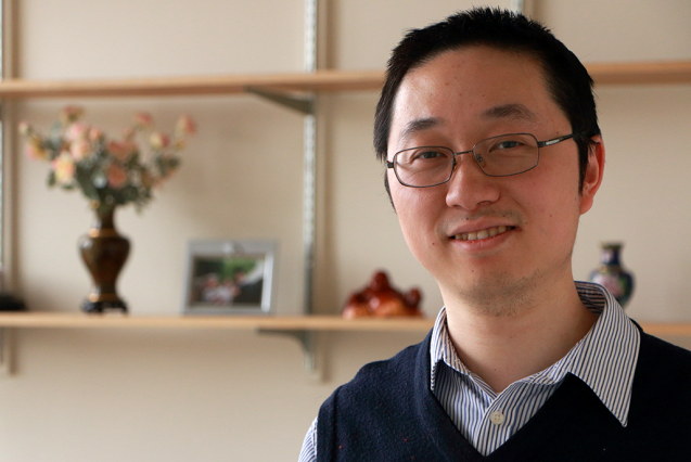
MIT Assistant Professor Juejun Hu melds fundamental materials science and new device designs to enable flexible photonics and other applications.
A special class of glass materials known as chalcogenide glasses holds promise for speeding integration of photonic and electronic devices with functions as diverse as data transfer and chemical sensing. Juejun "JJ" Hu, the Merton C. Flemings Assistant Professor in Materials Science and Engineering, is finding new ways to deploy these glasses with surprising flexibility.
Like regular glass, chalcogenide glasses are brittle, but Hu and colleagues developed a way to embed very thin glass photonic devices such as flexible microdisk resonators and waveguides in alternating layers of soft and stiff polymers. Their flexible plastic device sustained being bent thousands of times in a fatigue test without failing. And it demonstrated record optical performance, according to their 2014 paper in Nature Photonics.
"The structures that we made can be folded in half with an effective bending radius as small as 0.3 millimeter," explains Hu, who joined the Department of Materials Science and Engineering at MIT as assistant professor in January. "You can bend them by thousands of times without breaking and without seeing performance degradation as well."
Sandwich-cookie structure
Hu suggests one way to think of the device arrangement is to imagine a sandwich cookie with alternating hard and soft layers. "Instead of having one slab of material that has the same mechanical properties, we make a three-layer structure, with a very soft layer sandwiched between two relatively stiff layers. Now when you bend it, what you are imagining is that we have a very soft layer in between the two stiff layers, so it's going to deform first and it's actually going to absorb almost all of the mechanical deformation," Hu explains.
The "multi-neutral axis design" lays out the device so there is no place where the threshold pressure needed to crack the glass is exceeded. "While the entire structure is mechanically deformed, you can always put the glass in a location where it's getting little stress, you have no force exerted on the glass. That's how we actually make an entire structure very flexible out of something that's brittle. So it's about engineering the layout of the device," Hu says.
While the glass is on the order of 1 micron or less in thickness, the polymers on which it is fabricated measure in tens of microns. "So you can easily handle it, and that substrate serves as what I talk about, the agent, to relieve the stress or the forces on the glasses," Hu explains. "The glass sits on the stiff layer, and then when it deforms, despite the large geometric deformation, there is actually very little stress exerted on the glass," he says.
Multi-neutral axis design can also be applied to other brittle materials, such as ceramics or metals. "Anything's that stiff, we can always make it very compliant that way," Hu says. He published the work while still at the University of Delaware, where he served as a tenure-track assistant professor for four years.
Hu has research collaborations with colleagues at MIT, the University of Delaware, the University of Central Florida, the University of Minnesota, the University of Texas at Austin, the University of Southampton, and Orlando-based IRradiance Glass Inc. Besides flexible photonic devices, their work has demonstrated on-chip optical isolators using magnetic oxides, mid-infrared spectroscopic sensors on infrared-transparent substrates, and low symmetry gratings for enhanced solar cell performance.
"My dream is to see some of the things I develop at MIT have an impact in the real world and benefit the society as a whole. That's why I am interested in entrepreneurship, to push them to application; that's what I think MIT is great at," Hu says.
Substrate-blind photonic integration
In earlier work with MIT professors Caroline Ross and Lionel Kimerling and Microphotonics Center Principal Research Scientist Anu Agarwal, Hu used high-temperature processing and multi-layer build up, etching, and cleansing using masks and optical lithography to produce on-chip resonators and glass-on-silicon resonators in the same way computer chips are fabricated.
But Hu's more recent work in flexible photonic devices developed new methods for solution-processing of chalcogenide glasses at much lower temperatures. This approach, which enables inorganic-organic hybrid photonic devices, can be used for multiple host compositions leading Hu to brand it "substrate blind photonic integration" in an October 2014 SPIE report.
A 2014 Advanced Optical Materials paper demonstrated optical waveguides, microring resonators, and optical gratings that were fabricated using solution processing. The researchers used a single-step nanoimprinting method to directly mold chalcogenide glass films into device shapes. The process eliminates extra pattern-transfer steps.
"We dissolve the glasses in organic solvents, then dip your substrate into the solution, so they get coated with a uniform layer of solution, and then you vaporize and dry out all the residual solvent," he explains. It's a process that would be difficult with silica, he says.
Solution processing opens new possibilities for integrating glass photonic devices, which are inorganic, with organic-based polymer substrates versus traditional silicon substrates. The hybrids combine the superior optical properties of inorganic materials with the processing versatility of organic polymers. "Silica is one of the basic constituents of window-pane glasses. If you want to deposit silica, it has to be high temperature. At high temperature, you either cook the polymers or you destroy the underlying device you have on your substrate. Our glasses don't have that concern. You can put them on any substrate and will still maintain the integrity of the structure you have," Hu says. "It means that you can deposit the glasses on any substrate and make functional devices out of them without having to worry about whether your next layer is going to destroy what you already have on the substrate."
What makes chalcogenide glasses so different is that they replace the oxygen in familiar window pane glasses with "chalcogen" elements from the periodic table, principally sulfur, selenium, and tellurium. Their chemical compositions can vary substantially, yielding differing properties, but chalcogenide glasses share an affinity for transmitting infrared light, potentially enabling a host of commercial applications.
"By changing composition, you can tune the optical properties, so they are transparent to different wavelengths. You have freedom to tune the optical properties by adjusting the composition and without compromising the glass stability," Hu says.
"We also work on the fundamental materials science that allows us to develop new glass materials, for example," Hu explains. "Some of the new material we developed, we can actually hybridize the glasses with polymer materials." Hybridization enables new materials that both transmit light very well and confine light very well. "On the polymer side, they are extremely versatile in terms of how you actually process them or structure them into functional shapes," he says.
Hu has a long relationship with Irradiance Glass Inc. as a supplier for chalcogenide glasses, and Irradiance collaborators include Kathleen Richardson and J. David Musgraves. "They custom-make the special composition glasses, and we actually make them into the devices and test them. So they give [us] the raw materials; we developed the process to make them into devices and look at applications," Hu explains.
A bit of serendipity
When Hu's team began solution-processing chalcogenide glass materials, they found that the glasses could be processed at the same time with polymers, without degrading the polymer properties. "So that's where we came up with the idea, well we may as well use it to actually bring in the flexibility of polymers to make flexible devices," he explains.
"What initially happened was we had a project to process these glass materials from solutions instead of using conventional vapor-based deposition methods. One interesting characteristic that we found in the process is this entire process is very low-temperature. You can do it below 150 degrees Celsius, for example. At that time we started thinking about, well, this low temperature processing may have some benefits when you apply to different substrate materials, for example, polymers. And that's where we decided, it's an interesting direction, we should proceed," he says.
Mid-infrared sensing
Hu collaborated with University of Minnesota Assistant Professor Mo Li to develop a mid-infrared spectroscopic sensor that can detect chemicals with high performance. Reported in a 2014 ACS Nano paper, the device captures the position and resonant intensity of a special absorption light to identify chemical species such as ethanol and toluene.
"Ultimately we want to replace the benchtop spectrometer with something that can be integrated on a small silicon chip," Hu explains. "It's smaller, consumes much less power, and is actually a lot more sensitive, because we can pack in some new optical designs that allow us to enhance interaction between the molecules and the light." The sensor is a silicon photonic device on a substrate of crystalline calcium fluoride (CaF2). The researchers say calcium fluoride is highly transparent from visible light up to the mid-infrared wavelength of 8 microns. "Compared with other mid-IR photonics platforms including silicon-on-sapphire and germanium-on-silicon, silicon-on-CaF2 offers both a broad transparency window and the highest index contrast," they report. The researchers have several patents using the glass materials for mid-infrared platforms, which include infrared sensors.
Hu was a co-author on a 2011 Nature Photonics letter that demonstrated on-chip optical isolation featuring a magneto-optical garnet film coated onto a patterned silicon resonator. The researchers, including lead author Lei Bi and senior authors Ross and Kimerling, said the monolithically integrated device demonstrated an "ultracompact footprint, high isolation ratio, homogeneous magnetic field operation and controllable magneto optical dispersion."
Improving optical isolators
Hu says he and Ross have students working to improve performance of their optical isolator, a device that lets light travel in only one direction. "Dr. Ross developed new magneto-optical materials, and I work with new device designs. So together, we are hoping that we can improve the device so it achieves commercial-grade performance," he says.
"A lot of the projects are still in the research stage, but I'm interested in commercialization of the technologies once we have sufficient performance that will be able to compete with sustaining technologies."
Hu, 32, received his doctorate at MIT under Kimerling and completed his undergraduate work at Tsinghua University in Beijing, China. He is married and his wife also works in the Boston area. Hu's hobbies include reading science fiction, surfing the Internet, playing soccer with friends and watching soccer games. "It's really exciting to come back home. MIT is kind of like my home," he says
After joining MIT in January, Hu is in the process of relocating his Photonic Materials Group from the University of Delaware to MIT. There are eight students in the group, three who are MIT students and five who will complete their research at MIT but receive their PhDs from the University of Delaware.

 Previous page
 Back to top


