Better
understanding the science that underpins well-known techniques for developing
quantum dots—tiny semiconducting nanocrystals—can help reduce the guesswork of
current practices as material scientists use them to make better solar panels
and digital displays.
Just billionths of a meter across, quantum dots are routinely prepared in solution and coated or sprayed as an ink to create a thin electrically conducting film that is used to make devices. "But finding the best way to do this has been a matter of trial and error," says material scientist Ahmad R. Kirmani. Now, with colleagues at KAUST and the University of Toronto, Canada, he has revealed why certain well-known techniques can dramatically improve the film's performance.
Quantum dots absorb and emit different wavelengths of light depending on their size. This means they can be tuned to be highly efficient absorbers in solar panels, or to emit different colors for a display, just by making the crystals bigger or smaller.
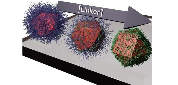
The dots are commonly grown from lead and sulfur in solution. Because the dots' properties depend on their size, their growth must be halted at the right point, which is done by adding special molecules to cap their growth. Engineers often use molecules of oleic acid, each with 18 carbon atoms, which attach to the crystal's surface, like hairs, blocking growth.
This creates a solution of dots suitable for coating to create a film. Yet, this film is not good at conducting electricity because the long acid molecules hamper the flow of electrons between nanocrystals. So engineers add shorter molecules. These "linkers" only have around two carbon atoms per molecule. The linkers replace the long capping molecules, increasing conductance. "The method has been used for a couple of decades, but nobody had investigated exactly what happens," says Kirmani.
To find out, Kirmani's team used a microbalance to monitor the exchange of oleic acid for linkers during the transition. They measured the spacing between the dots by scattering X-rays from them, and they also recorded the film's changing thickness, density and optical absorption characteristics.
Rather than seeing a smooth change in the film's properties, they saw a sudden jump—marking a phase transition. When roughly all the acid molecules have been displaced by linkers, the dots abruptly come close together, and the conductivity shoots up.
Kirmani hopes other teams will be inspired to investigate further, possibly by arresting the transition process somewhere midway and introducing various molecules to the dot surface to see what novel features emerge. "There is a lot of potential in taking this understanding to new paradigms for new technologies," he says.

 Previous page
 Back to top


