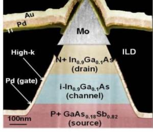
A new type of transistor that could make possible fast and low-power computing devices for energy-constrained applications such as smart sensor networks, implantable medical electronics and ultra-mobile computing is feasible, according to Penn State researchers. Called a near broken-gap tunnel field effect transistor (TFET), the new device uses the quantum mechanical tunneling of electrons through an ultrathin energy barrier to provide high current at low voltage.
 Penn State, the National Institute of Standards and Technology and IQE, a specialty wafer manufacturer, jointly presented their findings at the International Electron Devices Meeting in Washington, D.C. The IEDM meeting includes representatives from all of the major chip companies and is the recognized forum for reporting breakthroughs in semiconductor and electronic technologies.
Tunnel field effect transistors are considered to be a potential replacement for current CMOS transistors, as device makers search for a way to continue shrinking the size of transistors and packing more transistors into a given area. The main challenge facing current chip technology is that as size decreases, the power required to operate transistors does not decrease in step. The results can be seen in batteries that drain faster and increasing heat dissipation that can damage delicate electronic circuits. Various new types of transistor architecture using materials other than the standard silicon are being studied to overcome the power consumption challenge.
"This transistor has previously been developed in our lab to replace MOSFET transistors for logic applications and to address power issues," said lead author and Penn State graduate student Bijesh Rajamohanan. "In this work we went a step beyond and showed the capability of operating at high frequency, which is handy for applications where power concerns are critical, such as processing and transmitting information from devices implanted inside the human body."
For implanted devices, generating too much power and heat can damage the tissue that is being monitored, while draining the battery requires frequent replacement surgery. The researchers, led by Suman Datta, professor of electrical engineering, tuned the material composition of the indium gallium arsenide/gallium arsenide antimony so that the energy barrier was close to zero -- or near broken gap, which allowed electrons to tunnel through the barrier when desired. To improve amplification, the researchers moved all the contacts to the same plane at the top surface of the vertical transistor.

 Previous page
 Back to top


