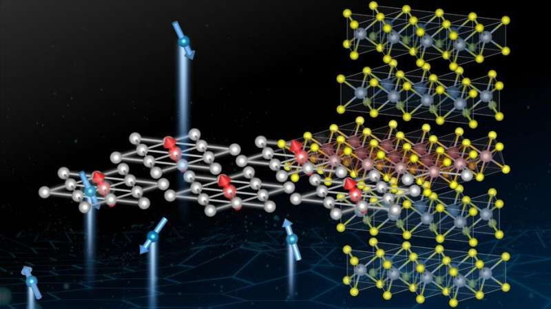
An international team led by EPFL
scientists, has unveiled a unique quantum-mechanical interaction between
electrons and topological defects in layered materials that has only been
observed in engineered atomic thin layers. The phenomenon can be reproduced by
the native defects of lab grown large crystals, making future investigation of
Kondo systems and quantum electronic devices more accessible.
The properties of materials that are technologically interesting often originate from defects on their atomic structure. For example, changing the optical properties of rubies with chrome inclusions has helped develop lasers, while nitrogen-vacancy in diamonds are paving the way for applications such as quantum magnetometers. Even in the metallurgical industry, atomic-scale defects like dislocation enhances the strength of forged steel.
Another manifestation of atomic-scale defects is the Kondo effect, which affects a metal's conduction properties by scattering and slowing the electrons and changing the flow of electrical current through it. This Kondo effect was first observed in metals with very few magnetic defects, e.g. gold with few parts per million of iron inclusions. When the diluted magnetic atoms align all the electrons spin around them, this slows the electrical current motion inside the material, equally along every direction.
Since it was described by theoretical physicist Jun Kondo in 1964, the topic has seen several revivals, and nowadays the effect is observed in many systems, from carbon nanotubes to superconductors.
A new perspective
Now, a team led by Professor Laszlo Forró at EPFL, has published a paper with a new perspective on the Kondo effect, made possible using the most advanced material characterization tools and microfabrication technologies available.
The scientists investigated the impact of magnetic defects, responsible for Kondo scattering, which are produced by atomic-thin planes in a layered material. Because of thermodynamics, the thin planes take an anomalous atomic configuration.
Such defects are intrinsically non-magnetic, but at low temperatures the electrons self-organize their spin within the defective layers producing a local magnetic planar defect inside the material.
Until now this configuration has only been created and studied in unique and custom-made samples either through manual stacking of atomic-thin layers of different materials or by expensive molecular beam epitaxy technology where materials are created atom-by-atom in an ultra-high vacuum.
The study used the innovative Focused Ion Beam microfabrication method developed by Professor Philip Moll and his team at EPFL, enabling the first experimental evidence of the anomaly in electronic transport properties.
The discovery that such phenomena can be produced by native defects, opens a new and more accessible way to explore unique quantum interactions in materials, which could boost discovery and transfer to technological solutions.
'Apply a magnetic field and see what happens'
"Once we first identified the anomaly in electronic conductivity, we remained very puzzled," says Edoardo Martino, the study's first author. "The material was behaving like a pretty standard metal whose electrons move along the plane, but when forced to move between planes its behavior became that of neither a metal nor an insulator, and was unclear what else to expect. It was thanks to a discussion with our fellow colleagues and theoretical physicists that we were pushed in the right direction: just apply a magnetic field and see what happens."
After applying the magnetic field, the EPFL scientists realized that the more powerful the magnet, the more exotic the material's behavior becomes. They started experimenting with 14 Tesla (460,000 times Earth magnetic field) superconducting magnets available at EPFL, but soon they realized they needed more.
Working with the Laboratoire National des Champs Magnétiques Intenses in Grenoble and Toulouse, they accessed some of the world's most powerful magnets. The collaboration performed experiments up to 34 Tesla in static conditions and with pulses up to 70 Tesla for a few milliseconds.
"My first guess was that it is a new type form of Kondo effect, despite the fact that we did not introduces magnetic species in the crystal," says Konstantin Semeniuk, a scientist who worked on the study.
"Once we completed our investigation, the result was clear," says Martino. "The atomically thin defects create a sort of magnetic wall in the material that bounces back some of the electrons that try to cross it. Unraveling the source of the Kondo effect has shown that thermodynamics can make big surprises. We believe there is a lot more to discover in this field, better understanding of atomic-scale defects by electronic microscopy, local magnetic measurements, and new quantum simulations to understand the formation and effect of such defects in layered materials."

 Previous page
 Back to top


